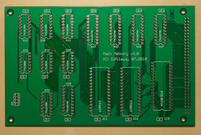
The base memory PCB described in one of the previous posts arrived in mail a week ago. The manufacturing and shipping process took BatchPCB (and USPS) exactly three weeks. Not bad, considering my design was first delivered to them on-line, then they had to lay out an entire panel of other peoples’ designs, then the panel was sent to China to be produced, returned from China in a batch delivery, and finally was shipped by BatchPCB to Poland, straight to by mailbox. Surprisingly, I received not one but two identical boards (although I paid for only one). I found out later that this is what BatchPCB guys often do – when there is some space on the panel, they duplicate some boards to fill it. So, there is often a chance of receiving a free bonus.
The board itself looks of decent quality (although I have zero experience, so my judgement may be misleading). I am not finding any discontinuities, and layers look well aligned. If my design is correct, it should work fine. Here is a close-up shot:

There is only one thing I am not particularly proud of – the trace width. I used Eagle auto-router with a setting of 8 mils, but by looking at the board now I think I could have used a wider trace, say 10 or 12 mils. The board density did not require me to use such high precision (traces look really thin). First lesson learnt – always check your routing grid density options, never assume you need to go as low as 8 mils.
I am still struggling to complete my main CPU board wiring, so the PCB will have to sit and wait for another while. Then, before starting the ALU board, I will take a short break from wiring and solder it. I already have a required set of precision sockets, some neat ceramic capacitors, and the connectors. All I need is a little more free time (this is always the hard part). With a CPU base board and the memory I should be able to run a set of tests and exercise a few basic instructions fetched from real RAM. Can’t wait.