My memory system has recently undergone an update to hardware design. Originally I planned and implemented four memory bank registers – two for lower and upper 32kB of code, and two for lower and upper 32kB of data (see this post for details). With hardware able to address maximum of 128 banks via 22-bit address bus, this results in total addressable physical memory of 4MB (128kB of ROM in banks 0..3, and 3968kB of RAM in banks 4..127). Banks configuration was controlled by four system registers (accessible only from supervisor mode):
| Address | Register |
| $2000 | REG_CODEPAGE0 |
| $2200 | REG_CODEPAGE1 |
| $2400 | REG_DATAPAGE0 |
| $2600 | REG_DATAPAGE1 |
Memory banks configuration was partly shared between user and supervisor modes, with the exception of lower code and data banks which in supervisor mode were hardwired to bank 0 and 4, respectively (first page of ROM and first page of RAM). This was sufficient for simple applications, but may cause me a lot of trouble soon when I try to run more complicated software, exercising switching between modes with access to arbitrary memory locations in both (e.g. when loading user programs in memory and launching them, or when servicing device interrupts in which quick access to memory is required). It also has a serious drawback of hardwiring lower page of supervisor’s code to ROM (something which is desirable, but only during system startup). Ultimately, I would like to have true memory paging, but I am currently not very enthusiastic about the idea of re-thinking and rebuilding the memory system completely. So, I decided to go for a quick fix which should give me more flexibility and programming comfort. The idea is to have not four but eight memory bank registers, and control supervisor and user mode memory setup independently:
| Address | Regsiter |
| $2000 | REG_SUPER_CODEPAGE0 |
| $2200 | REG_SUPER_CODEPAGE1 |
| $2400 | REG_SUPER_DATAPAGE0 |
| $2600 | REG_SUPER_DATAPAGE1 |
| $2800 | REG_USER_CODEPAGE0 |
| $2a00 | REG_USER_CODEPAGE1 |
| $2c00 | REG_USER_DATAPAGE0 |
| $2e00 | REG_USER_DATAPAGE1 |
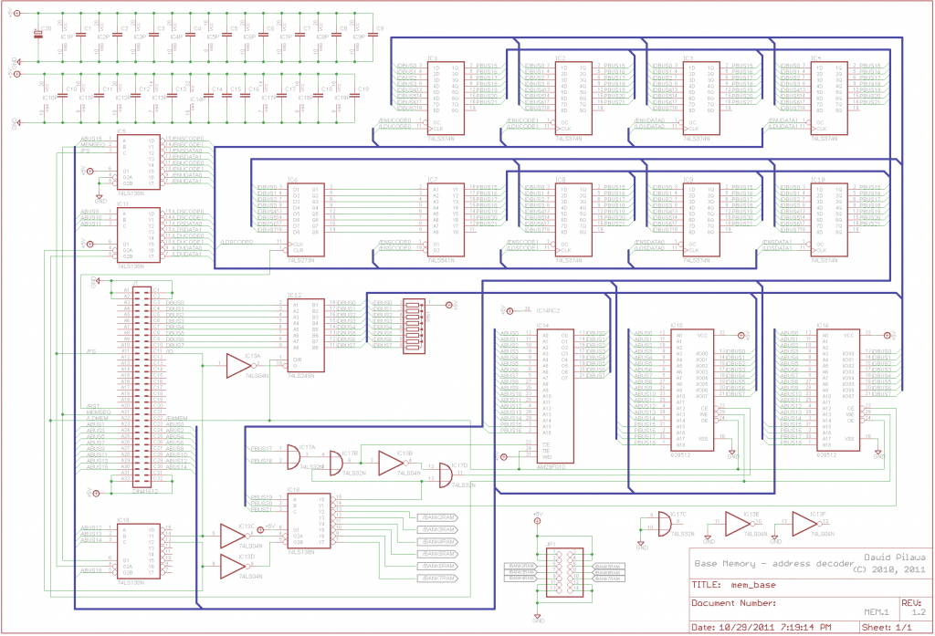
With this approach I had to assure that supervisor code page #0 register (REG_SUPER_CODEPAGE0) would be always reset to 00h on startup. Previously, with this value hardwired I did not have this problem at all. On startup the computer always executed code from first bank of ROM. Now, since first page of supervisor code is controlled by a writable register, I had to make sure my computer would boot properly. So, I built this one register using a 74LS273 with active low reset input and a 73LS541 three-state driver.
Although the new memory system seems a very simple change conceptually, when I looked at the schematic sheets I immediately realized that the update would require a major rework. So, I spend an evening and created Base Memory rev. 1.2 schematics, which does not resemble rev. 1.1 at all:
Note that I have also changed the 64-pin generic connector to a DIN-41612. The latter connectors seem to me more reliable and are definitely easier to plug and unplug, which in my case is a big benefit. DIN-41612 Type C is now my choice and I am going to use it for backplane connector all my boards. Tomorrow, I am planning to lay-out a new memory board and send it for manufacturing. I will then publish the new revision of entire schematics package.
