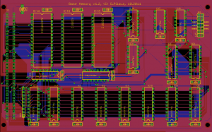
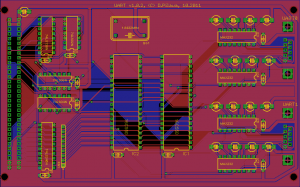
It is difficult to lay out boards properly. This task requires a lot of patience and experience, otherwise you end up with poorly routed boards, hundreds of vias or lengthy signal traces. Somehow I am still unable to avoid all these imperfections and my boards are not quite how I would like them to be. This time, I had to route not one but two new PCBs – one for a new memory system described in the last post and one for the UART controller and ports (I decided the design is stable enough to get its own custom board). The final result is below (click images to enlarge).
In general my PCB design approach requires the following sequence of steps:
- Place components on a board so that air-wires to connected components are as short as possible, but keep the layout clean (for some reason I do not like non-uniform placement of components).
- Route power lines of greater width (I use 40 mil traces). I do not route ground because I add a ground plane in the last step of the process. I attempt to route the power bus in the outer regions of the board, but it is not always possible (there are components in the center of the board, too and I need to reach them).
- Manually route critical traces like buses, traces to passive components or connectors. I like to have buses as bunches of parallel lines, not randomly placed traces as the autorouter tends to route them.
- Use Eagle autorouter to route remaining signals.
- Add ground plane on top and bottom side of the board (with Eagle’s orphans option disabled and thermals option enabled).
I try to keep the baseline layout from before the autorouter step to be able to make adjustments. This makes the process iterative – whenever I am not happy with the final layout, I undo the autorouter step, fix the component or power trace placement and hit autoroute again. All in all it costs me several man-hours to complete a board I am reasonably happy with. I think my major weakness is the second step – power lines routing. I need multiple attempts to do it more or less properly, without obstructing the way for other important signals and over-complicating the board. I even changed the pad shape from ellipses to smaller squares to save some space for signal traces but it did not help much. I still think I could have obtained a board with fewer vias and lower overall trace length, had I routed power lines better. Any hints how this should be done properly for two sided rectangular boards with through-hole components?
I have already sent the boards for manufacturing. choosing BatchPCB again for their unbeatable $2.50 per square inch plus $10 setup fee. I have also uploaded new schematics PDF and eagle files into downloads.

