BYTEC is undergoing a hardware revision and will soon receive a set of new features. Recently, while fiddling with monitor/OS and thinking what it would take to implement memory management in Minix, I realized that BYTEC’s memory system is way too simplistic and would lead to serious limitations. So, BYTEC/16 rev 2.0 is on its way, featuring a brand new MMU.
Memory Management Unit (MMU)
Current revision of BYTEC has no real memory management unit (MMU), and only a very simple paging circuit is implemented directly on the memory board. It divides code and data memory segments into two 32kB pages each, independently for supervisor and user modes. Pages are controlled by eight registers, accessible in data segment of supervisor mode at following addresses:
| Address range | Register | R/W |
| 0x2000-0x21FF | REG_SUPER_CODEPAGE0 | W |
| 0x2200-0x23FF | REG_SUPER_CODEPAGE1 | W |
| 0x2400-0x25FF | REG_SUPER_DATAPAGE0 | W |
| 0x2600-0x27FF | REG_SUPER_DATAPAGE1 | W |
| 0x2800-0x29FF | REG_USER_CODEPAGE0 | W |
| 0x2A00-0x2BFF | REG_USER_CODEPAGE1 | W |
| 0x2C00-0x2DFF | REG_USER_DATAPAGE0 | W |
| 0x2E00-0x2FFF | REG_USER_DATAPAGE1 | W |
I made the registers write-only to simplify the circuit. For the same reason I mapped them quite sparsely in memory, effectively occupying 4096 bytes of supervisor data segment, instead of just 8 bytes.
Making these registers write-only was good for hardware simplification and saved a few chips, but it was not the smartest design choice. While it would be acceptable (and even necessary) for memory manager in OS to maintain a per-process page table and store dynamic information about pages allocation, I have found it impossible for the OS initialization routines to determine in which physical pages the OS itself has been loaded into. This complicated building an initial free pages map, actually making it impossible unless an assumption was made that OS always resides in a hard-cored physical memory region.
More importantly, current hardware is not able to support demand paging or copy-on-write, both essential for a multitasking OS. It is assumed that pages selected by the above hardware registers are always present and always writable in physical memory. That is not always effective (program needs to be loaded to memory entirely, even if a small portion of code actually gets executed) and not always desired (you may wish to let programs run in same memory range only until one of them needs to write to it). Typically, this is solved by using dedicated page status flags and fault signals asserted on specific conditions (memory faults). I neither had the flags nor the signals. Even if I had, the fault mechanism of microcode sequences was not flexible enough to handle memory faults correctly (more on this later).
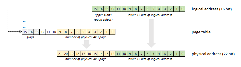
And so a plan was born – BYTEC/16 rev 2.0 will get a Memory Management Unit (MMU). The MMU will be another CPU card, and will handle all memory management logic internally to the CPU (avoiding a need to expose fault signals or alike on an external bus). The CPU with MMU will only present a 22-bit physical address bus to a simplified memory card which becomes merely a set of memory chips with no address translation logic. Address translation will be done by the MMU via a programmable page table implemented as fast SRAM array and residing in supervisor memory at address 0x0080-0x00FF (so occupying only 128 bytes in lower memory region, above the interrupt and fault vector). MMU will be enabled via a dedicated flag (/FP) of the machine status word (MSW register), a low active bit 6. With MMU disabled, logical address will be just passed through to a physical bus.
Each of the 64kB memory segments (supervisor code, supervisor data, user code and user data) will be divided into 16 pages of 4kB. Each of the 64 page entries will be 2 bytes long, hence 128 bytes of page table in total. To be more specific, this represents the following page table map in supervisor data memory:
| Address range | Contents | R/W |
| 0x0080-0x009F | 16 supervisor code page entries of 2 bytes each | R/W |
| 0x00A0-0x00BF | 16 supervisor data page entries of 2 bytes each | R/W |
| 0x00C0-0x00DF | 16 user code page entries of 2 bytes each | R/W |
| 0x00E0-0x00FF | 16 user data page entries of 2 bytes each | R/W |
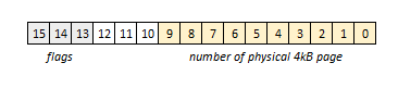
Each page table entry is 16 bits long, and is writable and readable. First (least significant) 10 bits determine a physical 4kB page number, allowing for 1024 pages, or 4MB physical memory in total. Last (most significant) 3 bits represent memory page flags:
Address translation itself is fairly simple – physical address will be created by taking 12 bits of logical address as least significant bits, and 10 bits from the respective page table entry as most significant bits (for a given memory segment and CPU mode). Page table entry will be selected using 4 most significant bits of logical address, and two bits representing current memory segment (CODE, DATA) and CPU mode (supervisor, user).
Meaning of the flag bits in page table entry is the following:
- Bit 15 – PRESENT bit, determines if a page is present in physical memory. Typically this is needed when a physical memory page has been previously swapped to disk and is again made available to a process (lazy swapping), or has never been loaded in order to save on disk I/O (lazy program loading). System should fault when such memory page is accessed, memory manager in OS will read the missing page from disk to memory and then return back to process.
- Bit 14 – WRITABLE bit, determines if a page may be written to. Here, a typical use case is a copy-on-write implementation when a process is forked. Once forked, new process gets initially the same memory segment but with disabled WRITABLE bit. This is OK as long as the new process does not write to memory. As soon as it attempts to write, the system faults, memory manager allocates a new page to the process (this time with WRITABLE bit on), copies the contents of old process’ page, and returns.
- Bit 13 – IO bit, determines if a particular memory page is a devices page. This means that device memory regions used by UARTS, RTC or IDE which were previously hard-wired in memory region 0x1000-0x1fff have now relative addresses mappings within the devices page and the whole I/O memory page can be mapped wherever the OS wishes. Although risky, such devices page may even be made available to a user mode program if an IO bit is on for a user page table entry.
All bits are used in hardware signals which are low active (so in this case zero means “on”). Bits 10..12 of page table entry remain unused, or can be used by OS for other purposes.
With the above address translation mechanism in place, one remaining problem to be solved is how to determine which memory page was accessed, when the system detects one of the fault conditions. It is not sufficient to check which instruction was last executed, because one instruction may access different memory regions (pages) in different microinstruction steps, e.g. POP A fetches a value from data memory at current stack pointer (1st memory read) and then fetches the next instruction from code memory (2nd memory read). To solve this, I have added another hardware register which is only loaded on memory fault (page_not_present or page_not_writable) and stores currently accessed memory page number (4 most significant bits of logical address in bits 0..3) along with CODE/DATA and SUPERVISOR/USER flags (bits 4..5), with remaining bits hardwired to zero. The register is accessible (read-only) to a fault handling routine under address 0x0020-0x0060 just above the interrupt vector (okay, I know I wasted 63 bytes of memory again but here the saving would not be worth the extra gates and unnecessary propagation delay, and 63 bytes is not 4kB after all).
Better faults
I mentioned that my faults mechanism was not capable of correctly handling memory faults. The following problems disqualified the former approach and called for a redesign:
- On fault, hardware would not store the current microinstruction step and whole instruction would be re-run upon return from fault handling routine. This was wrong as previous microinstructions may have had side effects (advancing stack pointer, reading from read-once device register and alike) and should not be repeated. Control should return to the microinstruction step which triggered a fault. Only the faulting and following steps should be re-run once fault condition has been removed. To fix this, I added a microinstruction step store (cache) register.
- There was no instruction to return from fault handling routine which would be able to restore the value from the new cache register. I ended up adding a new instruction FRET analogous to IRET only with an extra microcode sequencer control signal not to reset the microinstruction step but to restore it from a cache. In order to implement FRET I had to go back to microcode sources and microcode assembler, otherwise not touched in 3 years. I also had to sacrifice the HALT instruction because I have ran out of opcodes long time ago. This should not be a big issue, and I can always halt the machine by disabling interrupts and going into an endless loop in supervisor mode.
- On fault, instruction would fall through all its microcode steps until it encountered a fetch microinstruction. During this run, all signals able to modify registers or memory would be inhibited, so this did not constitute a similar problem to re-running the microcode steps from before the fault, but was an unnecessary waste of CPU cycles. I fixed that too by re-working the microcode sequencer’s glue logic.
Fault mechanism redesign was a rather trivial change. I could have done those things in my original design, but I never really gave it a better thought as (unlike for interrupts) I had not seen any real use for faults before looking into MMU topic.
What next?
I am currently finalizing schematics and board layouts, and will be able to share them here in one-two weeks, together with updated microcode and microcode assembler. As far as boards are concerned, in total I have touched 5 out of existing 7 CPU boards and added one new (the MMU), so BYTEC/16 rev 2.0 will consist of 8 boards in total. There will also be a completely new (although very simple) memory card. At this point I am not sure yet which fab house I will chose, but in any case there will be 3-4 weeks wait time which I will use for parts sourcing and updating documentation on this site, so I guess I will revert back to software in the meantime.
Hi Dawid,
Interesting approach!
Was this worth the effort?
intel 8086 and MC68000 did not have memory management and still got reasonable software and operating software, e.g. early UNIX, MINIX …
Thanks for your comments,
BR Fritz