Back from a 3-week long vacation in Cuba. Time to get back to work.
As mentioned before, the machine will be a typical CISC with a wide microcode word, with little encoding. That means that bits from microcode ROM will be directly used as control signals. This is in contrast to a RISC-like approach, where microcode words are compact and highly encoded, with microcode bits having different meaning for various instruction types with lots of additional hardware logic to decode them and generate actual control signals.
With this in mind, there are still many approaches I can follow to organize my microcode sequencer. I am considering two. One involves using an additional microcode step counter (iterating through microcode words within a machine instruction) and the other with a next field as part of microcode word (pointing to next microcode word’s address in microcode store). Both have advantages and both have some drawbacks. Here is how I see it.
Microcode step counter approach

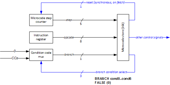
In this architecture, there is a dedicated counter register (the microcode step counter) used to iterate through the instruction’s microinstructions. The counter bits and instruction register (opcode) bits are concatenated to form a direct address to microcode store. In the diagram above, a 5-bit counter is indicated giving a maximum of 32 cycles per instruction. Using a 4-bit counter would result in instruction lengths of up to 16 cycles, which could be insufficient for complex instructions like faults, interrupts or supervisor/user context switches. Of course this also means that even the simplest instructions will use 32 lines of microcode space, with most microcode lines left unused. On instruction boundaries, the counter would be simply reset by one of the control signals of fetch microinstruction.
To handle conditional branches, microcode selects one condition from condition codes generated elsewhere, which (when latched) is used as a branch bit. With 3 condition select bits 7 different conditions may be supported (one of the conditions is reserved for always-true). The presence of branch bit means that the microcode store needs to be further divided into two halves – one used when an indicated condition is not met and other when it is met (branch occurs). This way, each microcode line (step) would exist in two versions. In most cases, with branch condition set to hardwired zero, both would be the same (or simply the latter would be irrelevant and could be random bits). Unused ROM space again.
Seems like it is would be simple to build and debug but there is something here I don’t like. This approach requires a lots of wasted microcode store and does not facilitate reusing microcode snippets (e.g. fetch microcode word needs to be repeated for each of the instructions). It would require 8+5+1=14 microcode addressing bits and RAM chips of 16kB (plus maybe some more bits and storage to handle faults and interrupts). With modern flash EPROMs cheap and easily available it seems not a problem but I have the feeling it is not the way it should be done.
‘Next’ field approach

This approach uses a ‘next’ field as part of the microcode word to indicate an address of the next microcode word. With this field and conditional branching mechanism it’s easy to write reusable microcode snippets and organize the microcode store densely (as they used to do it in the 70s and 80s).
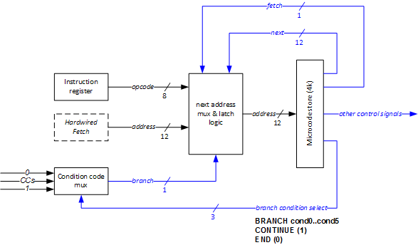
Here, there is no counter. Instead, we use some multiplexing and latching logic to determine the next microcode word address. Inputs to this logic block are hardwired fetch, instruction register contents (zero filled) and the current microcode word’s next field. Branch and fetch are signals used to select one of the inputs.
Each microcode word contains three branch condition bits, used to select between predefined conditions (up to 6) and CONTINUE or END special conditions. The condition code mux outputs a state of a selected condition, or CONTINUE (hardwired one), or END (hardwired zero). This state is used in next address mux & latch logic to select between the value of the ‘next’ field as indicated in the microcode word (when logic one) or a hardwired address of a fetch microinstruction (when logic 0). Hence, CONTINUE and END mean unconditional branch and unconditional fetch, respectively. Instruction register (IR) contents are not used here (fetch control line is not asserted). On a conditional branch condition code mux outputs the logic value of a selected condition code, and the resulting behavior is identical to CONTINUE (branch to the address indicated in ‘next’ field) or END (fetch the next instruction, do not branch). Note that we always fetch the next instruction when branch condition is not met – there is no way to fall through and simply execute next microinstruction word as there is no microinstruction counter.
Fetch microinstruction is slightly different and uses the additional fetch control line. Without going into details, when the fetch line is asserted the contents of the instruction register (zero filled to extend to microcode address width) are used as the next microcode word address. Branch control line is irrelevant in this case. Note that first 256 addresses of microcode ROM are also first microcode words for each of the instructions, and any subsequent words are stored somewhere in the ROM and reached by unconditional branches.
In this approach I could use a 4k microcode ROM. This gives me on average 16 steps (cycles) for each – more than enough, considering microcode reusability this scheme allows. However, this means also that I have to use 12-bits of each microcode word for the next field. That will require more ROM chips than in the first approach, and more board space. Moreover, 12-bit address size is a little awkward and will be ineffective to select and latch (more chips here, too). Certainly, 8 bits would be nicer but I am not sure I could fit into microcode space that small. Or, maybe? Bill Buzbee managed in his Magic-1.
Conclusions?
There are two ways to go now. Today, the latter seems more elegant to me (not as brute force as the step counter approach) and only a little more difficult to build.
Next, I need to think how to incorporate faults and interrupts mechanisms into the concept, so my next post should be on that, unless I change my mind with the approach, or I start thinking about memory organization, or microcode word, or something else.
Mr. Pilawa …
For the sake of my question assume a very simple “Microcode step counter approach” with a 4 bit Instruction Register and 4 bit Microcode Step Counter and no Condition Mux.
Stored in the Microcode Store (EPROM) would be something like:
Instruction IR Step Control Signals
Inactive State 0000 0000 Base State
LDA 0001 0000 PC’>MAR
0001 0001 PC counts
0001 0010 M’>IR Control signal to Load IR
0001 0011 PC’>MAR
0001 0100 PC counts
0001 0101 M’>MAR
0001 0110 M’>A
0001 0111 Reset Reset Step Counter
STA 0010 0000 to 0111
ADD 0011 0000 to 1000
SUB 0100 0000 to 1000
HLT 0101 0000 to 0011
How does the system move from on one Instruction to the next? Such as from the Inactive State to LDA or from LDA to ADD. In the LDA example above, the Instruction Register will need to have 0001 … but the fetch instructions are not completed until the thrid clock cycle when the control word to load the IR is activiated.
Thanks,
Randy
First of all you have to keep in mind that in this approach the pair (IR, step) always defines the absolute address to your microcode store. So, you cannot just load the IR in the middle of microcode execution of a particular instruction (this way you will break the execution), but only at the very end (i.e. when you are done with whatever the instruction is supposed to do). This loading of the IR occurs when PC already points to the next instruction address and is done together with resetting the step counter (in order to start the next intruction’s execution from its very first step). This operation is called ‘fetch’ as part of a typical instruction cycle composed of ‘fetch’, ‘decode’ and ‘execute’ operations. In the approach I am suggesting, ‘fetch’ is always the last step of instruction execution. In your example, the microcode for LDA would be something like:
0001 0000 load A with memory content at PC; advance PC
0001 0001 load IR with memory content at PC; advance PC; reset counter
With a design smiilar to mine, this can be done in just two cycles. The second microinstruction is a ‘fetch’. After ‘fetch’, the counter will be set to zero, IR will contain the opcode for the next intruction to execute, and PC will point to the operand of the next instruction. Care needs to be taken so that the PC is always one step in front (note that I advanced PC in step 0000 to meet this requirement). As an effect, the system moves from one instruction to the next. Hope this helps.